
品牌说明
本型号为 AVAGO(安华高) 产品。安华高与博通(Broadcom)属于同一家公司:安华高 2005 年由安捷伦分拆上市,2016 年被博通收购,成为博通旗下半导体业务,业内常以 AVAGO/安华高/博通 混称。本页参数与规格书均取自该产品线原厂资料。
产品应用与封装尺寸
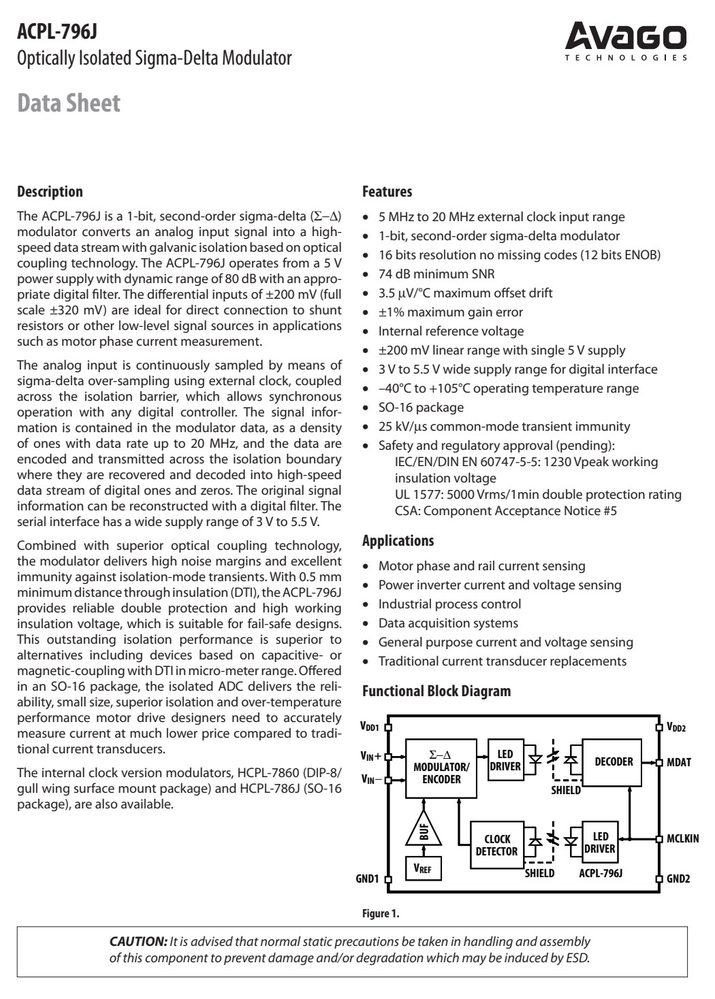
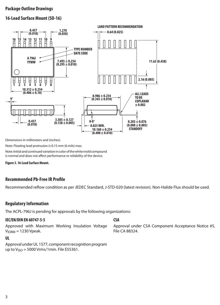
图纸取自原厂规格书,点击可放大查看原始尺寸标注。
引脚定义与内部结构
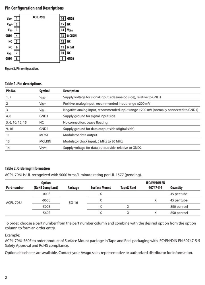
| 引脚 | 符号 | 名称 |
|---|---|---|
| 5 | V | |
| 6 | V | |
| 7 | V | |
| 10 | NC | |
| 11 | MDAT | |
| 12 | NC | |
| 13 | MCLKIN | |
| 14 | V | |
| 15 | NC |
数据来源:原厂规格书引脚图
关键参数速览
- 正向电流 IF
- 1. Data changes at the clock
- 隔离电压 VISO
- 25
- 电源电压 VCC
- 6.0
- 工作温度 TA
- 40 to 105
产品特点 Features
- 5 MHz to 20 MHz external clock input range
- 1-bit, second-order sigma-delta modulator
- 16 bits resolution no missing codes (12 bits ENOB)
- 74 dB minimum SNR
- 3.5 V/°C maximum offset drift
- ±1% maximum gain error sion modes (combinations of speed and resolution), three different pre-trigger modes (allows conversion time
- <1 s), offset calibration, fast over-range (over-current, or short circuits) detection, and adjustable threshold modulator without additional hardware. Refer to the
- HCPL-0872 data sheet for details.
- Notes:
- SPI and QSPI are trademarks of Motorola Corp.
- Shunt Resistors
- The current-sensing shunt resistor should have low re- sistance (to minimize power dissipation), low inductance
- Smaller shunt resistances decrease power dissipation, while larger shunt resistances can improve circuit accuracy by utilizing the full input range of the isolated modulator.
- The first step in selecting a shunt is determining how much current the shunt will be sensing. The graph in
- REWOPESROH
- 35 380
绝对最大额定值 Absolute Maximum Ratings(TA = 25°C)
超过下表数值可能造成器件永久损坏,设计时请留余量。
| 参数 | 符号 | 最小 | 最大 | 单位 |
|---|---|---|---|---|
| Storage Temperature | T | –55 | +125 | °C |
| Ambient Operating Temperature | T | –40 | +105 | °C |
| Supply voltage | V , V DD1 DD2 | –0.5 | 6.0 | V |
| Steady-State Input Voltage[1,3] | V +, V – IN IN | –2 | V + 0.5 DD1 | V |
| Two-Second Transient Input | Voltage[2] V +, V – IN IN | –6 | V + 0.5 DD1 | V |
| Digital Input/Output Voltages | MCLKIN, MDAT | –0.5 | V + 0.5 DD2 | V |
| Lead Solder Temperature | 260°C for 10 sec., | 1.6 mm below | seating plane |
数据来源:原厂规格书
安全与绝缘额定值(DIN EN/IEC 60747−5−5)
| 说明 | 符号 | 值 | 单位 |
|---|---|---|---|
| Installation classification per DIN VDE 0110/1.89, | Table 1 | ||
| for rated mains voltage ≤ 150 Vrms | I-IV | ||
| for rated mains voltage ≤ 300 Vrms | I-IV | ||
| for rated mains voltage ≤ 450 V rms | I-IV | ||
| for rated mains voltage ≤ 600 Vrms | I-IV | ||
| for rated mains voltage ≤ 1000 Vrms | I-III | ||
| Pollution Degree (DIN VDE 0110/1.89) | 2 | ||
| Input to Output Test Voltage, Method b | V | 2306 | Vpeak |
| V × 1.875 = V , 100% Production Test | with t = 1 sec, | ||
| Partial Discharge < 5 pC | |||
| Input to Output Test Voltage, Method a | V | 1968 | Vpeak |
| V × 1.6 = V , Type and Sample Test, t = | 10 sec, | ||
| Partial Discharge < 5 pC | |||
| Highest Allowable Overvoltage (Transient | Overvoltage, t = 60 sec) V | 8000 | Vpeak |
电气特性 Electrical Characteristics(TA = 25°C)
| 参数 | 符号 | 最小 | Typ.[1] | 最大 | 单位 | 测试条件 | 图号 |
|---|---|---|---|---|---|---|---|
| A | DD1 | DD2 IN | |||||
| Resolution | 16 | Bits | Decimation filter output set to 16 bits | ||||
| Integral Nonlinearity | INL | –15 | 3 | 15 | LSB | T = –40°C to +85°C; see Definitions | section |
| –25 | 3 | 25 | LSB | T = 85°C to 105°C | |||
| –25 | 25 | V + = –250 mV to +250mV | |||||
| Differential Nonlinearity | DNL | –0.9 | 0.9 | LSB | No missing codes, guaranteed by | design; | |
| see Definitions section | |||||||
| Offset Error | V | –1 | 3 | 4.5 | mV | T = –40°C to +105°C; see Definitions | section |
| Offset Drift vs. | TCV | 3.5 | V/°C | ||||
| Offset Drift vs. V | 120 | V/V | |||||
| Gain Error | G E | –2 | 2 | % | T = –40°C to +105°C, V + = –250 to A IN | +250 mV; | |
| see Definitions section | |||||||
| –1 | 1 | % | T = 25°C, V + = –250 to +250 mV | ||||
| Gain Error Drift vs. | TCG | 60 | ppm/°C | ||||
| Gain Error Drift vs. V | 110 | V/V | |||||
| Full-Scale Differential | FSR | ±320 | mV | V = V + – V –; Note 2 | |||
| Average Input Bias | Current I | –0.5 | A | V = 5V, V = 5V, V + = 0 V; Note | 3 6 | ||
| INA | DD1 DD2 IN | ||||||
| Average Input | Resistance R | 33 | k | Across V + or V – to GND1; Note 3 | |||
| Input Capacitance | C | 8 | pF | Across V + or V – to GND1 | |||
| DYNAMIC CHARACTERISTICS | V + = –200 mV to +200 mV, 543 Hz, | sine wave; Note 4 | |||||
| Signal-to-Noise Ratio | SNR | 74 | 80 | dB | T = –40°C to +105°C; see Definitions | section | |
| Signal-to- | SNDR | 65 | 75 | dB | T = –40°C to +105°C; see Definitions | section 7, 8 | |
| 68 | 75 | dB | T = –40°C to +85°C | 7, 8 | |||
| 65 | T = –40°C to +105°C, V + = –250 mV | to +250 mV 7 | |||||
| Effective Number of | Bits ENOB | 12 | Bits | see Definitions section | |||
| Isolation Transient | Immunity CMR | 25 | kV/V | V = 1 kV; See Definitions section | |||
| Common-Mode | Rejection CMRR | 74 | dB | ||||
| Input High Voltage | V | 0.8 × | V | Note 5 | |||
| Input Low Voltage | V | 0.2 × | V | Note 5 | |||
| Input Current | I | ±0.5 | A | ||||
| Input Capacitance | C | 6 | pF | ||||
| Output High Voltage | V | V | V | V | V = 5 V supply, I = –200 A | ||
| OH | DD2 | DD2 | DD2 OUT | ||||
| V | V | V | V = 3.3 V supply, I = –200 A | ||||
| DD2 | DD2 | DD2 OUT | |||||
| Output Low Voltage | V | 0.4 | V | I = +200 A | |||
| V Supply Current | I | 14 | 19 | mA | 9, 10 | ||
| V Supply Current | I | 6 | 8 | mA | V = 5 V supply | 11, 12 | |
| DD2 | DD2 | DD2 | |||||
| 5 | 7 | mA | V = 3.3 V supply DD2 | ||||
| 1. All Typical values | are at T = 25°C, V | = 5 V, V | = 5 V. | ||||
| 2. Beyond the full-scale | input range the | data | output is either | all | zeroes or all | ones. | |
| 4. Signal frequency | of 543 Hz is used as | a reference | frequency | for | coherent | sampling. | |
| Unless otherwise noted, | T = –40°C to +105°C, | V = | 4.5 V to | 5.5 V, V | = 3 V to | 5.5 V. | |
| Modulator Clock Input | Frequency f | 5 | 10 | 20 | MHz | Clock duty cycle 40% to | 60% |
| Data Delay After Rising | Edge of t | 3 | 15 | ns | C = 15 pF | 5 | |
| Input-Output Momentary | V | 5000 | Vrms | RH ≤ 50%, t = 1 min; | 1, 2 |
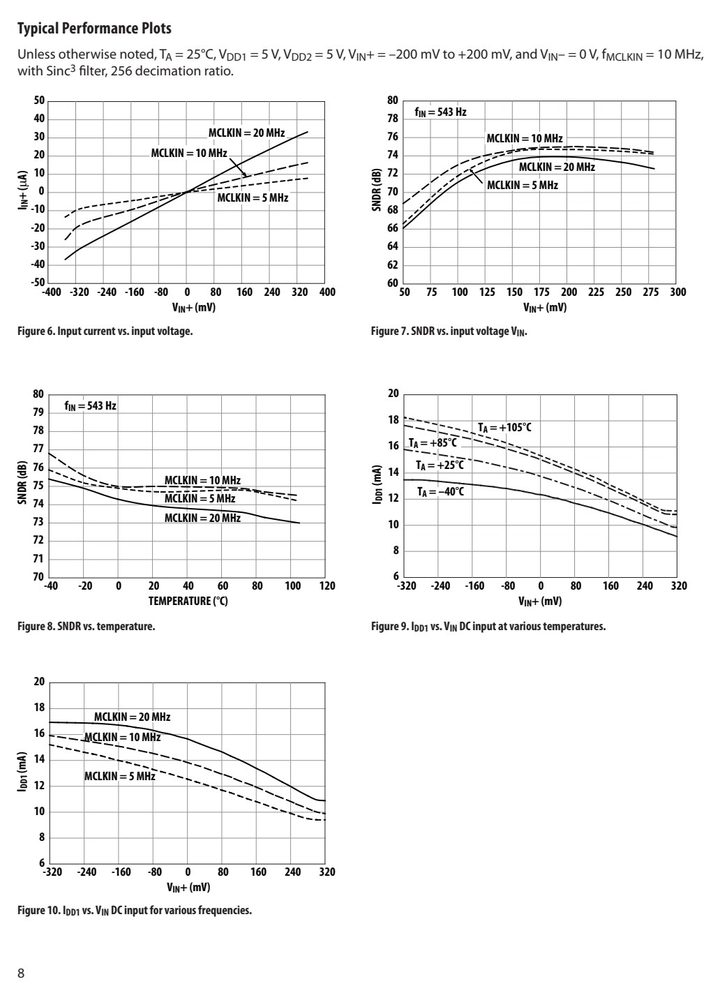
特性曲线(Typical Performance Curves)
应用领域 Applications
获取报价 / 申请样品
常备现货、免费送样、支持小批量试产。报出用量与封装要求,当天给报价与交期。
销售直线(点击可直接拨打)📞0755-82811939点击拨打📞0755-82812373点击拨打📞0755-82811915点击拨打📞0755-82811193点击拨打企业 QQ(点击跳转对话)💬QQ 2850611261企业QQ 对接💬QQ 2355817597企业QQ 对接💬QQ 3002728093企业QQ 对接💬QQ 2355817598企业QQ 对接
手机端点号码直接拨号/唤起 QQ;电脑端点座机会唤起系统拨号应用,点 QQ 会打开企业QQ 对话窗口。